

Services
SERVICESContact Us
CONTACT USZHUHAI KAMEDA TECHNOLOGY CO., LTD.
Tel: +86 756 516 6177
Email: Show contact details
Add: 4/F, Block 4, No.26 XinKe 2nd Rd, Baijiao Science & Technology Industrial Park, Doumen District, Zhuhai, Guangdong, China 519100
+86 756 516 6177
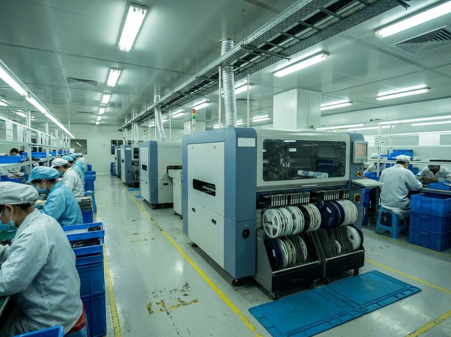
SMT is the main process here. Three lines, fine pitch, QFN and micro BGA, with the smallest part placed 01005 imperial (0402 metric) and 0201 imperial (0603 metric) as standard. Boards run from standard FR-4 through aluminium (MCPCB), ceramic, Rogers, flex and rigid-flex. Prototype, pilot run and volume production go through the same equipment and the same inspection.
Surface-mount parts sit on pads on the board face: paste holds them until reflow, and the reflowed joint holds them afterwards. No hole is drilled for the lead, which is what allows tighter pitch, smaller packages and placement on both sides.
Through-hole leads pass through plated holes and are soldered on the far side. The joint is stronger under vibration and repeated mating, so transformers, large electrolytics and connectors keep that format. Most real products carry both: reflow first, then through-hole and secondary soldering. Both processes run in this building, so a mixed-technology board never leaves the site mid-build.
Capability
| Placement capacity | Three SMT lines with a combined rated placement capacity of 500,000 components per hour |
| Smallest component | 01005 imperial (0402 metric), with 0201 imperial (0603 metric) as standard |
| Packages | QFP, SOP, QFN, BGA, micro BGA, CSP, fine-pitch devices |
| Placement format | Single-sided, double-sided, and mixed SMT plus through-hole |
| Board types | FR-4, aluminium (MCPCB), ceramic, Rogers, flex, rigid-flex |
| Board construction | Multilayer, HDI, blind and buried vias, controlled impedance |
| Board size | Set against your panel drawing; tooling rails and panelisation agreed at engineering review |
| Stencils | Laser-cut stainless steel, nano-coated where fine pitch and micro BGA need a clean release |
| Soldering | Reflow, wave and selective soldering |
| Solder alloy | SAC305 lead-free as standard; tin-lead where you specify it. |
| Rework | BGA rework and IR rework at a dedicated station |
| Inspection and test | Solder paste inspection, AOI, X-ray, ICT, flying probe, FCT, visual inspection |
| Workmanship | Boards are built to the IPC-A-610 acceptance class you specify. State Class 2 or Class 3 on the RFQ. |
| Workshop | Temperature and humidity controlled, ESD-controlled floor |
Panel size, board thickness and component height are confirmed board by board at engineering review rather than published as a blanket limit, because the answer depends on the carrier, the pallet and the profile the board needs. Send the panel drawing with the RFQ and you get the figure for your board before you commit to the layout.
Process
- Paste printing: laser-cut stencil, thickness and apertures set from pad size and board thickness, nano-coated where fine pitch or micro BGA needs a clean release. Squeegee pressure, print speed and separation speed are set per board. Paste is stored refrigerated, and warm-up and stir times are recorded before use.
- Solder paste inspection: volume, offset and slump are checked after printing. An out-of-range print stops the line and the stencil or the parameters are corrected there, not downstream.
- Placement: our SMT lines run the board single- or double-sided, with fine-pitch and micro BGA parts placed on vision centring rather than package outline. The program and the first article are checked together for reference designator, orientation and polarity.
- Reflow: the profile is built inside the paste supplier’s window and confirmed with a thermocoupled board. Ramp rate, soak, time above liquidus and peak are measured on the real assembly before the batch runs. Heavy copper and aluminium boards get their own profile.
- AOI: every board is checked for missing, wrong and reversed parts, offset, bridging and insufficient solder. Failures go to the rework station and the defect is logged by reference designator.
- Test: hidden joints under BGA, micro BGA and QFN go through X-ray. The board then takes ICT, flying probe or FCT as ordered, and a visual check before packing.
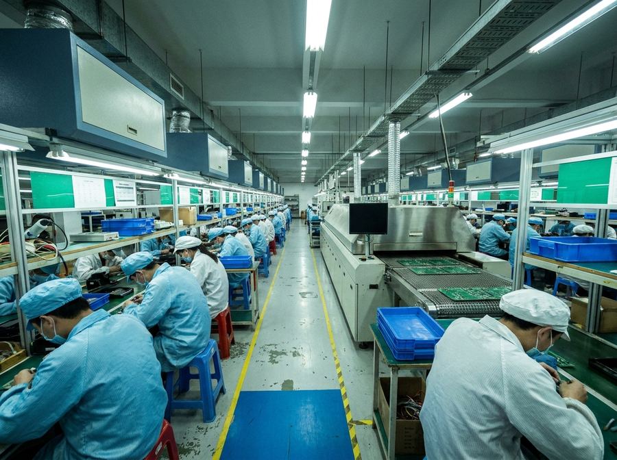
Inspection and test
- Solder paste inspection (SPI): after printing, before placement. Catches paste volume and registration problems while they are still cheap to fix.
- AOI: after reflow, and after printing where the board warrants it. Wrong part, offset, tombstoning, bridging, insufficient solder.
- X-ray: BGA, micro BGA, QFN and any joint that cannot be seen. Voiding, bridging, opens and head-in-pillow.
- ICT: bed-of-nails fixture, measuring in-circuit values. Finds opens, shorts and wrong parts quickly on volume runs.
- Flying probe: no fixture to build, so it suits prototypes and small batches. Opens, shorts and basic component values.
- FCT: functional test against your test specification, on your fixture or one we build, with the board under simulated operating conditions.
- Visual inspection: every board before packing, for appearance, markings, joint formation and cleanliness. Records stay with the batch.
Preventing the common defects
Solder balls
Solder balls come from too much paste, slump between printing and reflow, or a preheat ramp fast enough to boil off flux volatiles and throw solder powder clear of the pad. Apertures are sized to the pad rather than copied from the footprint, pulled back at the ends of chip components with home-plate or reduced openings, and squeegee pressure and separation speed are held to the values set for that board. The preheat ramp is kept gentle, paste is brought to room temperature before the jar is opened, and stencils are wiped on a fixed print count.
Bridging
Bridging appears on fine-pitch QFP and QFN leads and traces back to excess paste volume, oversized or badly shaped apertures, placement force squeezing paste out from under the lead, and slump between print and reflow. Apertures are narrowed to lead width and shaped to keep paste out of the gap, SPI holds deposit volume before anything is placed, placement force and nozzle choice are set for the package rather than left at the default, and every board goes through AOI after reflow. Where the joints sit under the package, X-ray confirms them instead of AOI guessing at them.
Cold joints and opens
Cold joints, non-wetting and opens usually come from oxidised pads, paste past its working life, poor lead coplanarity, or a skipped print. Paste is stored refrigerated with warm-up and stir recorded, incoming inspection samples pad condition and lead condition, SPI catches the thin or missing deposit before placement, and BGA and QFN joints are confirmed by X-ray rather than assumed good because the board powered up.
Tombstoning
Tombstoning happens when the two terminations of a chip component reach liquidus at different moments and the wetting force on the first end lifts the part. Most of the fix is in DFM: pad symmetry, thermal relief and copper balance are checked at engineering review, and we tell you which footprints we want changed and why. On the process side the soak is lengthened so both terminations arrive at temperature together before the reflow segment starts.
Head-in-pillow
Head-in-pillow is a BGA joint where ball and paste deposit both melt but never merge. It can pass continuity today and open on the next thermal cycle, which makes it the expensive one. Causes are package or board warpage at reflow temperature, oxidised balls, weak flux activity and thin paste deposits. Moisture-sensitive devices are handled to their MSL rating with floor time logged and baked when the level requires it, paste volume is held by SPI, the profile is tuned to limit time at peak, and every BGA is X-rayed. If your package is known to warp, say so at review and we will settle aperture and profile changes before the first build.
Each countermeasure is written into the work instruction and process sheet for that board, proved on the pilot run and frozen before volume starts. Production defects are recorded by reference designator and batch, so a repeat order does not repeat the investigation.
For a quotation, send us your Gerber, BOM and pick-and-place files — we reply within one working day.